> ## Documentation Index
> Fetch the complete documentation index at: https://docs.deneyapkart.org/llms.txt
> Use this file to discover all available pages before exploring further.
# Warnings (DYG)
## Pin Conflicts
* During code (firmware) upload, do not make any external connections to the **D2 (BT)** pin. After the upload process is completed, you may make an external connection.
* While the built-in addressable RGB LED is in use, do not make any external connections to the **D3** pin.
* If an external connection is provided via the I2C connector, an external connection using an I2C interface with the same pin configuration may be made to the **D4 (SDA)** and **D6 (SCL)** pins; however, do not make any other external connections to these pins.
## Incorrect Pin Labeling
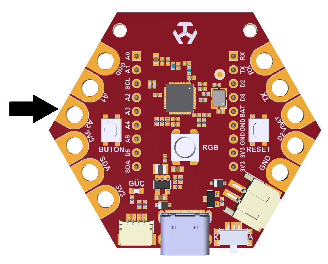
In the image below, the sewable pad marked is incorrectly labeled as **"A2"** on the board. The correct name of this pad is **"SCL"**.
 ## Maximum Voltage for Analog Reading
The **A0, A1, SCL, A2, A3,** and **A4** pins, which have **12-bit** resolution, can be used as input pins for analog signals. These pins reach the maximum value of **4095** at approximately **2.85 V**.
## Maximum Voltage for Analog Reading
The **A0, A1, SCL, A2, A3,** and **A4** pins, which have **12-bit** resolution, can be used as input pins for analog signals. These pins reach the maximum value of **4095** at approximately **2.85 V**.